Thursday, November 20, 2014

Audio Frequency Generator Circuit

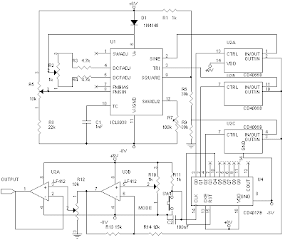
Audio Frequency Generator or often known by AFG is a device electronics used to generate signals with audio frequency range. Audio Frequency Generator (AFG) in the market there are many variant, from the analog to the digital . Even the assembly also exists, in principle, AFG is the frequency generator with an audio range. Here is one set of Audio Frequency Generator (AFG) which can be a reference if you want to make a series of Audio Frequency Generator (AFG) . The series of Audio Frequency Generator (AFG) is to use IC L8038 as a signal generator it.
Audio
AFG
The series of Audio Frequency Generator (AFG) above has three output waveform that is, sine, square and triangle directly from the IC L8038. IC CD4066 and IC circuit Cd4017 a configuration circuit for waveform selector that can be set by pressing SW1. To adjust the working frequency is set by potentiometer R2.
Read More..

2 Transistor Line Follower Robot

Make a line follower robot can be done with two transistors. Line Follower Robot series is one of the two transistors contor robot line follower circuit is in Bagun with two NPN transistor and the motor driver as well as processing of sensor signals.

In the circuit of line follower robot consists of two parts of the same, only different functions for the motor driver the right and left. Sensor circuit of line follower robot uses the LDR and LED. LDR sensor sensitivity can be set with the VR 10 is mounted in series with the LDR. For more details, see the following figure.

Line Follower Robot series 2 Transistor


The working principle of the motor driver circuit between the right and left together, when the LDR get the reflection of light from the LED LDR resistance will decrease and make the transistor saturation and motor gets supply and rotates so that the robot moves forward. So at the moment is not the case then the motor did not get a supply, for example, only one sensor is exposed line and make the LDR did not receive the reflected light is then Motr in the stationary and the other motor rotates and makes the LDR are back in the reflection of light and the robot moves forward again.

Line Follower Robot

Read More..

Wednesday, November 19, 2014

Adapter power supply and charger circuit

Basically adapter, power supply and charger circuit has a similar construction which consists of a transformer, rectifier (rectifier) and smoothing the voltage. For there is usually an additional power supply voltage stabilizer of voltage regulator IC LM series 78XX or 79XX .
Below is a schematic circuit adapter, power supply, or battery charger (for gadgets, mobile phones, MP4player, smartphone) that is equipped with a 5V voltage stabilizer:

Adapter, power supply and charger circuit

Read More..

USB SPDIF DAC with IC PCM 2902

The tool that I made and I discuss in this article I give the name USB SPDIF DACEvery word in the name corresponds to the function of the tool that I made this.

USB, this device serves to take the music information in digital form from a computer via the USB port
SPDIF, this tool can output digital music information received through the USB port, through the SPDIF output terminal that is also present in this device, so if you have a DAC that does not have a USB input, you can still use and do not need to buy a new DAC that has an input USB.
DAC, this tool can convert the digital signals derived from the USB port, an analog signal, which you can connect to the amplifier to the ahirnya you can hear the speaker

Scheme of the USB DAC can be seen in Figure 1 below.
Click to view larger. | Figure 1

As you can see on the schematic in Figure 1 above, which is the heart of the circuit is IC USB DAC PCM2902 made ​​by Texas Instrument, other than that I also added a digital SPDIF output isolation transformer on from this series. 2902 PCM encoding decoding work on the principle that generally abbreviated as word CODEC. 
The new circuit will work when the USB input port terminal in the circuit connected to the computer, at this voltage 5V on the USB port of any computer will be triggering the circuit to begin work, and vice versa when the computer is turned off then the circuit will be in standby mode to wait until there is more tension 5V from USB port of computer. 
When the received voltage is 5V USB port the computer then the circuit will begin to receive the digital data files during the grace period of 1 ms, all data received during the period of time of 1 ms is called a frame, the data in the first frame is stored in a memory buffer that is in the PCM2902, then the circuit will start the second frame as well as long lead times for 1mS, 1mS a second after the first data from the file will be converted into analog signals for analog terminal is then removed through out the pin 15 and 16 of the PCM2902, other than that this digital signal simultaneously will also excreted through the DOUT terminal pin 25 of the PCM2902 DAC to be connected to older products that do not have a USB input terminal.In addition to functioning as a DAC, PCM2902 actually also has other functions such as setting volume level and ADC, but the circuit that I developed is only aimed for the ADC and the conversion from USB to SPDIF.

Proposed Power Supply For USB SPDIF DAC
Power Supply that I use in this project using the configuration has been proven able to tame the hum in the tube 26, the power supply has karakater very stable, low noise and low impedance, but complicated to make, so for the purposes of this project I recommend another series that is not as complicated Heater power supply 26, but the quality is still better than most of the power supply kit used in the DAC in general, Figure 2 below is the recommendation power supply for USB DAC this project.
Click to view larger. | Figure 2

Power supply circuit in Figure 2 above is composed of four main parts, namely
 1. Diode bridge and capacitor input filter
 2. TL431 as the reference voltage
 3. OP Amp OP27 as the error amplifier
 4. BD139 transistor as a pass transistorThis configuration is basically the general configuration of a linear regulator series, very much the regulator IC using this configuration, but the circuit in Figure 2 above has several advantages that are not owned by the regulator circuit in the form of ICa) high stability, since it uses a reference voltage source of good quality is TL431, and therefore not in a package with a pass transistor, the heat of the pass transistor can not seep into the source of reference voltage and makes it unstable, this sort of thing happens in IC voltage regulator.b) Using the Op Amp high quality, which in this case OP27, so it is not easy to oscillate as the OpAmp used in the regulator IC.c) If there is a chance you could also replace the TL431 or OP27 Op Amp voltage source and another that is expected to be better than either of these components.
Series of the finished PCB, top view

IC PCM2902
Read More..

Tuesday, November 18, 2014

Different types of TV TUNER

TV tuner that is used on older models and new models of television there are some differences. Therefore, understanding the different types of tuner would be useful if we want to replace the tuner with the other models.
Supply voltage tuner.
Tuner older models generally use a supply voltage of 12v, the new models are commonly used 5V supply voltage. Some use a 9V voltage, but very rare.

TV TUNER
Voltage Synthesizer tuner (VS tuner)
Tuner that uses a tuning control (VT or BT) with a voltage between 0 to 33V Voltage Synthesizer tuner named. TV can be found on the aircraft models, old and new
Based on how the control band-switch, Tuner VS then there are 2 kinds, namely
Using 3-Band input sw, the VL-VH-U
Using 2-Band input sw, the Band SW1 and SW2 Band. This tuner is actually similar to the type of band 3-sw. For control-sw 2 band is in the tuner will still be converted into 3-sw bands.

Frequency Synthesizer tuner (FS tuner) or the type of PLL
Tuner wherein the tuning voltage and the voltage controlled band switching the digital communication through SDA and SCL. This tuner has a supply voltage Vcc, which is
5V is used for the digital tuner circuit control and
33V (fixed voltage or fixed) is used to control the voltage supplied to the tuning in the digital circuits within the tuner.
(Tuner old) sometimes there are additional circuit voltage of 12V to the tuner.

Frequency band.
Based on the wide range of revenue-frequency band, there are three kinds of tuner
Normal tuner
Superband tuner
Tuner hyperband

Normal tuner, the tuner that can receive broadcasts "on-air" (terrestrial) TV in the frequency band:
  • Frequency of VHF Band I - VL 41-68 Mhz
  • Band III - VH 174-230 Mhz
  • Frequency UHF Band IV - U 470-581 Mhz
  • Band V - U 582-960 Mhz
  • Band II 87.5 - 104 MHz is used for FM radio broadcasting
  • VL and VH bands used for broadcast channels 2 through 12
  • U bands used for broadcast channels 21 to 69
Superband Tuner and Hyperband, the tuner can receive broadcast as normal tuner plus the ability to receive broadcasts "off air" CATV (cable television).
  • S band using frequency band between VL and VH
  • H-band using a frequency band between VH and U
  • Superband Tuner can receive the broadcast band S
  • Hyperband tuner can receive broadcast band and S band H
Based on the IF frequency out
IF frequency tuner out there who have 38/38.9/45.75 Mhz frequency. In Indonesia generally use 38.9Mhz frequency, but sometimes there is a use 38.0Mhz


Based on the pin-out
There are several kinds of tuner long pin-out configuration. But now almost all the tuner is already using an international standard 11-pin

Universal tuner
China is now producing "universal tuner" 11-pin. Indonesia was just the market we do not know whether it exists or not. This tuner can be used to substitute for the various types of tuners and tuner can adjust to this direct voltage of 5, 9, or 12v.

RF antenna input connector
Form the antenna input connector there are two kinds, namely:
  • RCA type connectors
  • Antenna RF connector
Tuner modules
Tuner is a tuner module inside there are all Video IF amplifier circuit and the FM-detector. This kind of tuner is using VS and some are using the FS.
Tuner module has output like:
  • RF AGC-out
  • RF AFC-out
  • Audio-out
  • Video-out
  • Base band out, the signal to be processed into stereo sound circuit.
Except that in tuner is also sometimes diperlengkapa with audio-switch to TV / AV-in. Therefore, to the sound of the AV-in connected via Audio-in found on the tuner module. Sometimes the sound volume to be controlled in the tuner module.
  • SONY tuner module 1
  • SONY tuner module 2
  • Toshiba tuner module
Impedance input / output
Impedance tuner has all kinds of input / output 75 ohm.

How to distinguish 2-band tuners VS sw with PLL tuner FS
In all these circumstances and the removable pin 11 feet was not cut, it is sometimes difficult to distinguish between two band-tuner tuner sw with FS.
Some models have a tuner pin legs partially emptied. FS Tuner has a location pin 30V voltage 3 numbers from the back (of the IF pin out).
Read More..

Non Latching Momentary Switches


The most common are push-button, but toggle switches too may be spring-loaded to return to one position after activating. In the catalogues, an (ON)-OFF description means its only ON while youre holding the lever in place. With push-button, theyre more often described as momentary-on (push to make) or momentary-off (push to break). Heres how the two types could be used together to control ON-OFF action by latching a relay, a very common system on industrial control gear. The relay needs to have two or more poles (the switches) which can be change-over (double-throw) or single-throw types.

The "On" switch S2 is a push-to-make (momentary on) type, and allows power through to the relay coil when pressed. This becomes an electro-magnet and pulls all the relay switches over to the no (normally-open) position. (With relays, normally-open and normally-closed refer to the switch positions with no power applied to the coil.) Relay switch Sw2 now keeps power running to the relay coil after the "On" button has been released, latching the relay into the on position.

Relay switch Sw1 is used to switch power to whatever load you have attached, (Extra relay switches would be used, for example, to control a 3-phase electric motor.) Pressing the "Off" button S1, a push-to-break (momentary off) type, breaks the power circuit, deactivating the relay electro-magnet and sending its switches back to the nc (normally-closed) position. The diode D1 gives an easy path to any voltage spike produced when the relay coil turns off (back-EMF) protecting any sensitive equipment on the same circuit.
Read More..

Monday, November 17, 2014

Variable Switching Regulator Circuits

Switching Regulator Variable L4970 is supplying current to a maximum of 10A with an adjustable output voltage from 0-25 VDC. Switching Regulator Variable L4970 series is built with the main component as a Switching Regulator IC L4970 her. Switching Regulator Variable L4970 series include not complicated to make his own, which need to be considered is the IC L4970 require sufficient cooling to operate in an optimal and durable. Switching Regulator Variable Series L4970 complete picture can be seen below.

Variable Switching Regulator

Output Voltage Switching Regulator Variable L4970 series can be in control by adjusting potentiometer 18KOhm.
Read More..

5000W High Power Audio Amplifier

The High Power Amplifier has great advantages are 5000W ultra-light, high-power audio amplifier, without switching-mode power supply. This ambit is of an 2 x 2,500W RMS Stereo amplifier, super-light and after switching-mode ability supply. The ambit aloof shows a channel, and the ability accumulation that it assists to the two channels. The audio ambit should be duplicated, but the ability accumulation assists to the two channels after problems.
Click To view larger | 5000W High Power Amplifier Audio Circuits Diagrams

A adapted affliction should be destined to the careful agent of the audio line, that should be of audio-high-quality, of the blazon acclimated in microphone pre amps ascribe line. The accomplished accumulation (2 channels) of 5,000W RMS it should not counterbalance added than 32 lbs, already central of an adapted brownish box.

WARNING:
This ambit is alone for abecedarian use. It contains not-isolated genitalia of the electric AC net and it can be actual dangerous. The access for the speakers are not abandoned of the calm AC net and it requests added care. This action seeks to acting a accepted ability accumulation with abundant weight and amount reduction, after necessarily to use a switching-mode ability supply.

This action cannot be accustomed in some countries for commercial-use. The columnist doesn’t accept any albatross for the anatomy as that ambit it will be applied.
Read More..

Friday, November 14, 2014

FIRE ALARM CIRCUIT

It will detect the fire automatically and inform to the people with an alarm. Now-a-days, fire alarms are must for the apartments, theaters, hotels, restaurants, coal mines, petrol bunks or gas stations, etc.Here is the simple fire alarm circuits which will use different concepts and different components for generating the fire alarm. The main basic concept is almost same that sensing the fire or heat by the component and giving that information to the remaining circuit to give alarm.

This is a simple fire alarm circuit using Germanium Diode and 555 timer. In this circuit Germanium Diode play very important role in detecting the fire.This circuit is very easy to construct, cost effective and implementable.

Circuit Description

Here is the simple fire alarm circuit which costs less than 100 rupees. The key component in the circuit is DR25 (germanium diode) whose resistance will decrease with increase in temperature. The conduction of germanium diode will start at 70 degrees. So we may use germanium diode as a heat sensor. When the temperature is more than 70 degree, the germanium diode will conduct and trigger the NE555 timer through a transistor. The NE555 is configured in astable multivibrator and make the buzzer to alarm when germanium diode conducts. So that we can get alert and act according to the alarm.

Circuit Diagram


Circuit Explanation


  • The DR25 germanium diode is heat sensor which will conduct when temperature is increased at certain point. The DR25 is made reverse biased in the circuit. It will conduct only when it is more than 70degree of room temperature.
  • The DR25 is connected to the transistor in reverse bias, which has high reverse resistance (more than 10K ohm) and  does not make the transistor to turn off which is connected to the reset pin of 555 timer. The reset pin of 555timer will be in ground level when the transistor is turned off. Here, the 555 timer is configured as astable multivibrator.
  • When more than 70degrees in room temperature occurred, the resistance of DR25 diode drops to 1k ohm which will make the transistor to turn off and make the reset pin to go high. This will generate the output at pin3 and make the sound through the alarm.
  • We can use 3 or more diodes in reverse bias connected in parallel and placed in different room. If there is fire accident, it will sense and make the alarm.

Note 

  • If DR25 germanium diode is available, you can still use AC128, AC188 or 2N360 germanium transistors. Use base and emitter junctions in place of cathode and anode.
  • Diode must be connected to the circuit in reverse bias.
Read More..

Thursday, November 13, 2014

B5 Audi Radio System Schematic Diagram

Audi The following schematic shows the 1997 – 2001 Audi B5 Radio System Schematic Diagram. It consists of :

1. Radio
2. Bass Speaker
3. Mid-range/treble Speaker
4. Broad Band Speaker
5. Antenna Base
6. Roof Antenna
7. CD Changer
8. Bose amplifier combined with bass speaker (subwoofer)
9. Bass speaker (subwoofer) only with "concert" radio

Read More..

What is Schematic Diagram Definition

What is schematic diagram

Definition of schematic diagram: Schematic diagram is a visual presentation that describes the interconnection between device and power with enough detail to assemble an electronic circuit.

For example this is a schematic diagram of FM receiver:


schematic

And this is a block diagram of FM receiver:


block

 
Image credits goes to:
http://electroschematics.com & http://www.hobbyprojects.com
Read More..

Wednesday, November 12, 2014

NJU7365 bassed DC brushless motor driver circuit with explanation


A very simple single phase dc brushless motor driver electronic circuit project can be designed using NJU7365 DC brushless motor driver ic manufactured by New Japan radio Co. LTD .

The NJU7365 is a single phase motor driver ic that include in package MOS FET motor driver , direct PWM input , FG output and thermal shut down circuit . The driver is capable of 1000mA maximum output current and continuous current of 350 mA . This motor driver require few external electronic parts and can be powered from dc power supply from 2 to 5.5 volts .

Read More..

20 Watt Automotive Power Amplifier LM2005

The high current capability of the LM2005 allows it to continuously endure either AC or DC short circuit of the output with a maximum supply voltage of 16V. This will protect the loudspeaker in a bridge mode, when a DC short of the output occurs on one side of the speaker.


The device will prevent the speaker from destruction by reducing the DC across the load (bridge mode) to typically less than 2 VDC(VSe14.4V, RLe4X), by an internal current pullback method.

The LM2005 can withstand a constant 28 VDC on the supply with no damage (maximum operating voltage is 18V). The device is also protected from load dump or dangerous transients up to 40V for 50 ms (every 1000 ms) on the supply with no damage.The LM2005 is a dual high power amplifier, designed to deliver optimum performance and reliability for automotive applications. High current capability (3.5A) enables the device to deliver 10W/channel into 2X (LM2005T-S), or 20W bridged monaural (LM2005T-M) into 4X, with low distortion.Features
  • Wide supply range (8V±18V)
  • Externally programmable gain
  • With or without bootstrap
  • Low distortion
  • Low noise
  • High peak current capability
  • PO=20W bridge
  • High voltage protection
  • AC and DC output short circuit protection to ground oracross load
  • Thermal protection
  • Inductive load protection
  • Accidental open ground protection
  • Immunity to 40V power supply transients
  • Pin for pin compatible with TDA2005 (Datasheet)
Read More..

Tuesday, November 11, 2014

Loudspeaker Impedance Meter

Also suitable for Headphones Operates in conjunction with a DVM
A simple Impedance Meter can be useful to measure the actual impedance a loudspeaker or headphone is presenting @ 1kHz standard frequency. The circuit, designed on request, relies on an earlier design (Spot-frequency Sine wave Generator) to obtain a stable, low distortion 1kHz sine wave avoiding the use of thermistors, bulbs or any special amplitude-limiting device. The sine wave output, after some amplitude setting obtained by means of P1, is sent to the device under measurement through a resistor.

A regulated supply is necessary to obtain a stable output waveform. D1 and D2 force IC1 to deliver 6.2V output instead of the nominal 5V. The measurement is done in two stages: as a constant current supply of the device under test is necessary, this can be set at first by adjusting P1 and measured across the series resistor (R7 or R8, depending on the impedance value to be measured); then, the meter is switched across the device under test and the actual impedance will be read directly on the meter display.
Circuit diagram:
Loudspeaker Impedance Meter Circuit Diagram 
 
Parts:
P1_______________4K7 Linear Potentiometer
R1______________12K 1/4W Resistor
R2_______________2K2 1/4W Resistor
R3_______________1K 1/2W Trimmer (Cermet)
R4_______________1K5 1/4W Resistor
R5_______________4K7 1/4W Resistor
R6_______________3K3 1/4W Resistor
R7_____________100R 1/4W Resistor (See Notes)
R8_______________1K 1/4W Resistor (See Notes)
R9_______________1K 1/4W Resistor (Optional)
C1______________22nF 63V Polyester Capacitor
C2_____________330nF 63V Polyester Capacitor
C3______________22µF 25V Electrolytic Capacitor
D1,D2_________1N4148 75V 150mA Diodes
D3_______________3mm Red LED (Optional)
Q1,Q2,Q3_______BC550C 45V 100mA Low noise High gain NPN Transistors
IC1____________78L05 5V 100mA Regulator IC
SW1,SW2_________SPDT Toggle or Slider Switches
SW3_____________SPST Toggle or Slider Switch
B1________________9V PP3 Battery

Clip for PP3 Battery
Circuit set-up using an oscilloscope:

Connect the oscilloscope in place of the DVM and rotate P1 fully clockwise.
Short the speaker output and adjust R3 to obtain a sine wave of about 2.2V peak-to-peak amplitude.

"By ear" circuit set-up:

Connect a small loudspeaker or one of the two earpieces forming a pair of headphones to the circuit output and rotate P1 to obtain a moderate output sound level.

Carefully adjust R3 until the output sound will stop; then turn back the trimmer very slowly and stop adjusting immediately when the sound will start again.

Measurement:
  • Connect a Digital Voltage Meter set to 200mV ac range to the DVM output terminals
  • Connect the device under test to the Speaker terminals
  • Switch SW1 in the position towards R7 if the impedance value to be measured is below 100 Ohm or towards R8 if above
  • With SW2 in the "Set" position power-on the circuit by means of SW3
  • Adjust P1 in order to read exactly 100.0mV on the DVM display
  • Switch SW2 in the "Measure" position and read directly the loudspeaker or headphones impedance value on the DVM display, e.g. 8.5mV = 8.5 Ohm
  • Please note that when measuring devices with impedance values above 100 Ohm (SW1 set towards R8), the decimal point in the DVM reading must be ignored. E.g. if the display shows 70.5mV, the impedance will be 705 Ohm

Notes:
  • For very precise measurements use 1% or 2% tolerance resistors for R7 and R8.
  • D3 LED pilot light and its current limiting resistor R9 are optional.
Read More..

Sunday, November 9, 2014

Constructing a Universal Power Supply using LM317 Rise

This is a basic,  Universal Power Supply voltage regulator circuit using an LM317, 3-terminal regulator in a TO-220package. The Universal Power Supply output voltage can be set to anywhere in the range one.5V to 30V by selecting resistances. By using a potentiometer, R2, as of the resistors you can dial up the output voltage wanted. Either AC or DC input can be supplied to the PCB by a socket or terminal block. Connection can be either way around. This is because they have provided a bridge rectifier on board. The input DC voltage to the regulator must be at least two.5V above the necessary output voltage. An off/on switch is provided.

For lots of applications (say 12V at 60mA) a heat sink wont be required. The LM317 will provide slightly higher output voltages than 30 volts. However, for most hobbyists over 30V wont be needed. So to make a small PCB they have used some electrolytic capacitors rated to 35 volts. To be safe for continuous operation the maximum input DC voltage to the regulator ought to not be over 33V. With a two.5V to three.0V drop across the regulator this will give a regulated output of 30V. You can draw up to one.5A from the LM317. In case you need higher then use an LM338T rated to 5A.

When outside capacitors are used with any IC regulator it is lovely practice to add protection diodes to prevent the capacitors discharging back in to the regulator in the event of abnormal operating conditions, like a sudden short circuit on the input or the output, or a back emf from an inductive load. That is the function of D one and D Two.

The worth of R1 can range anywhere from 120R to 1200R However, circuits from most other sources settle on using either 220R or 250R. They have used 240R or 250R. The voltage drop across R1is one.25V for all values, and this is the key to the design. one.25V is the reference voltage of the regulator. Whatever current flows through R1 also flows through R2, and the sum of the voltage drops across R1 and R2 is the output voltage. (Additional current Id also flows in R2 but it is usually 50uA so is negligible.)

The design formula are:
VOUT = 1.25 (1 + R2/R1) volts, or alternatively
R2/R1 = (VOUT/1.25) - 1

So in case you know VOUT & R1 is 250R then you can calculate R2. In case you find that the 5K potentiometer used forR2 does not give you the degree of fine control over the voltage output range that you need then you can use these formula to fine-tune R1 & R2 to better suited values.


Universal Power Supply Schematic Diagram


Read More..

Saturday, November 8, 2014

Wire Loop Game

In the ‘Wire Loop Game’, a test of dexterity,  the player has to pass a metal hoop along a  twisted piece of wire without letting the hoop  touch the wire. Usually all the associated electronics does is ring a bell to indicate when the  player has lost. The version described here has  a few extra features to make things a bit more  exciting, adding a time limit to the game and a ticking sound during play. 

Two 555 timer ICs are used to provide these  functions. IC1 is configured as a monostable which controls the time allowed for the  game, adjustable using potentiometer P1. IC2  is a multivibrator to provide the ticking and Two 555 timer ICs are used to provide these  functions. IC1 is configured as a monostable which controls the time allowed for the  game, adjustable using potentiometer P1. IC2  is a multivibrator to provide the ticking and he continuous buzz that indicates when the  player has touched the wire with the hoop. 

Circuit diagram :

Wire Loop Game Circuit Diagram

When the monostable is in its steady state,  the output of IC1 (pin 3) is low. T1 acts as  an inverter, and D2 is thus forward biased.  R8 and R4 are therefore effectively in parallel, with the result that IC2 produces a low audible tone. The value of R4 is considerably  greater than that of R8, and so the frequency  of the buzz generated by IC2 is chiefly deter-mined by the value of R8.

When the monostable is triggered, the high  level at the output of IC1 is again inverted  by T1. D2 is reverse biased and so R8 is effectively removed from the circuit. The frequency of IC2 is now largely determined by  the value of R4. The ratio of R4 to R5 and the  value of C4 affect the mark and space periods for the multivibrator: for a satisfactory  ticking sound short pulses with long gaps  between work well. 

Whether a sound is produced also depends  on the voltage on pin 4 of IC2. When the 9 V  supply is connected the monostable is initially inactive and there is no voltage across  C1. Pin 4 (reset) on IC2 is thus low and no tone  is produced. IC1 is activated by a brief press of  S1, which generates a low-going trigger signal  on pin 2 to start the game. C1 now charges via  D1 and IC2 is allowed to oscillate, generating  the ticking sound. 

The pulse width of the monostable sets the  game duration, and can be adjusted using  P1. If the allowed time expires, or if the reset  input to IC1 is taken low (which happens when the hoop touches the wire), the monostable  returns to the quiescent state. This causes IC2  to generate the low buzz sound. D1 is now  reverse biased and C1 discharges through the  relatively high-valued resistor R9. After a few  seconds the voltage across C1 falls sufficiently  that the buzz stops and the circuit is ready for  the next player. 

The circuit can be built first on a breadboard,  so that the component values can easily be changed to suit particular preferences for  game duration and buzz pitch. When suitable  values have been selected the circuit can be  built more permanently on a printed circuit  board. The author used a sheet of plywood  to form a base for the game, the twisted wire  being fixed to the board and wired to the electronics mounted below it.
Read More..

Easy The flashing Heart

Buying a gift for someone special or a loved one can sometimes be difficult or expensive. The flashing heart is the answer. It is easy to build and even the inexperienced hobbyist should be able to build it. The estimated cost for the circuit is $25 if all the parts are purchased new. With The Flashing Heart, you can get your message across in bright lights.

The collectors of Q2 and Q3 are connected to R4 and R5 respectively, which are connected to the cathodes of the Yellow LEDs. Pin 13 is the oscillator output and is connected to R8, which is connected to the base of Q1. The collector of Q1 is connected to R3, which is connected to the cathodes of the Red LEDs. The emitters of the three transistors are connected to ground. The Green LEDs are connected to R1 and R2, which are connected to +12VDC. Resistors R1-R8 are current limiting resistors and the correct wattage for these resistors should be used to prevent excessive heat. The resistive values may be changed to vary the brightness of the LEDs. The circuit is powered by PS1, a wall transformer, which is connected to a filter capacitor C1. It must be between 10 to 15 VDC and at least 500mA.

Circuit Description The Circuit Diagram is shown in Figure 1. It consists of a 4047 low-power monostable/astable multivibrator, IC1, used in the astable mode to provide the timing pulses to control the flash rate of the LEDs. To accomplish the astable mode, pins 4, 5, 6, and 14 are connected to +12VDC and pins 7, 8, 9, and 12 are connected to ground. Pins 1 and 3 are connected to C2 and pins 2 and 3 are connected to potentiometer R9. A fixed value resistor can be used in place of the potentiometer R9, if the flash rate does not need to be adjusted. These three pins make up the R-C timing circuit. The output pulses from the 4047 are taken from pins 10, 11, and 13. Pin 10 is the Q output and pin 11 is the Q-not output. These two pins are onnected to R6 and R7 respectively.


Figure
Click On Image To Enlarge


Construction
Probably the most difficult part of this project is making the printed circuit board, Figure 2. The board used in the prototype took several hours to make using dry transfers. Using a different technique, such as photo resist, may be faster for the experienced hobbyist. Once the board is etched and drilled, the jumper wires should be placed on the board and soldered, as shown on Figure 3. Next the 84 Yellow LEDs should be placed around the border of the board, followed by the 42 Red LEDs that make up the heart and then the 16 Green LEDs that make up the letters I and U. Resistors R1-R9 and capacitors C1and C2 should be placed on the board next and then the power supply, PS1. Sockets were used in the prototype for the I.C. and transistors. A socket for the I.C. is required, but the sockets for the transistors are not. Special care should be taken when handling the CMOS I.C., as a static discharge will destroy it. When you are finished soldering, check the board over for mistakes. If everything looks okay, apply power.
Figure   Figure
Click On Images To Enlarge

Operation
Once power has been applied to the circuit, the Red LEDs should all be flashing on and off together. The Yellow LEDs should be flashing on and off, but only every other Yellow LED should be on at one time. The Green LEDs will stay on at all times. The flash rate can be adjusted by turning R9. Connections for a fixed value resistor for R9 are provided on the board layout if preferred.To dress up the project, a favorite photograph can be placed in the heart, and a frame can be made to fit the circuit board.

Parts List


Resistors
R1, R2 - 470 ohm, 1/2-watt
R3-R5 - 100 ohm, 3-watt
R6-R8 - 1000 ohm, 1.4-watt
R9 - 5000 ohm potentiometer


Capacitors
C1, C2 - 100uF, 16 volts, electrolytic radial


Semiconductors
IC1 - 4047, low power monostable/astable multivibrator
Q1-Q3 - 2n3643 NPN transistor or equivalent


Diodes

LED1-LED84 - yellow light-emitting diode
LED85-LED126 - red light-emitting diode
LED127-LED142 - green light-emitting diode


Other components
PS1 - 12VDC @ 500mA wall transformer


Miscellaneous: Jumper wire, solder, printed circuit board,
Read More..

Friday, November 7, 2014

Automatic Battery Charger Circuit Diagram

Normally, chargers available in the market do not have any sort of control except for a ro-tary switch that can select different tap-pings on a rheostat, to vary the charging current. This type of control is not adequate because of the irregular fluctuations in the mains supply, rendering the control ineffective.  A simple circuit intended for automatic charging of lead-acid batteries is presented here. It is flexible enough to be used for large capacity inverter batteries. Only the rating of transformer and power transistor needs to be increased.

Circuit diagram : 
Automatic Battery Charger Circuit Diagram
 
The circuit has been basically designed for a car battery (about 40 Ah rating), which could be used for lighting two 40W tube lights. The circuit includes Schmitt trigger relay driver,float charger,and battery voltage monitor sections.  The Schmitt trigger is incorporated to avoid relay chattering. It is designed for a window of about 1V. During charging, when the battery voltage increases be-yond 13.64V, the relay cuts off and the float charging section continues to work. When battery voltage goes below 11.66V, the relay is turned on and direct (fast) charging of the battery takes place at around 3A.  In the Schmitt trigger circuit, resistors R1 and R2 are used as a simple voltage divider (divide-by-2) to provide battery voltage sample to the inverting input terminal of IC1. The non-invert-ing input terminal of IC1 is used for reference input derived from the output of IC2 (7806), using the potentiometer arrangement of resistors R3 (18 kilo-ohm) and R4 (1 kilo-ohm). 

LED1 is connected across relay to indicate fast charging mode. Diodes D3 and D6 in the common leads of IC2 and IC3 respectively provide added protecion to the regulators.  The float charging section, comprising regulator 7812, transistors T3 and T4, and few other discrete components, becomes active when the battery volt-age goes above 13.64V (such that the relay RL1 is deenergised). In the energised state of the relay, the emitter and collector of transistor T4 remain shorted, and hence the float charger is ineffective and direct charging of battery takes place. 

The reference terminal of regulator (IC3) is kept at 3.9V using LED2, LED3, and diode D6 in the common lead of IC3 to obtain the required regulated output (15.9V), in excess of its rated output, which is needed for proper operation of the circuit. This output voltage is fed to the base of transistor T3 (BC548), which along with transistor T4 (2N3055) forms a Darlington pair. You get 14.5V output at the emitter of transistor T4, but because of a drop in diode D7 you effectively get 13.8V at the positive terminal of the battery. When Schmitt trigger switches ‘on’ relay RL1, charging is at high current rate (boost mode). The fast charging path, starting from transformer X2, comprises diode D5, N/O contacts of relay RL1, and diode D7. 

The circuit built around IC4 and IC5 is the voltage monitoring section that provides visual display of battery voltage level in bar graph like fashion. Regulator 7805 is used for generating reference voltage. Preset VR1 (20 kilo-ohm) can be used to adjust voltage levels as indicated in the circuit. Here also a pot meter arrangement using resistors R7, R8, and R9 is used as ‘divide by 3’ circuit to sample the battery voltage. When voltage is below 10V, the buzzer sounds to indicate that the safe dis-charge limit has been exceeded.
Read More..

Test Beeper For Your Stereo

The test beeper generates a sinusoidal signal with a frequency of 1,000 Hz, a common test  frequency for audio amplifiers.  It consists of a classical Wien- Bridge oscillator (also known as  a Wien-Robinson oscillator). The network that determines the  frequency consists here of a series connection of a resistor and  capacitor (R1/C1) and a parallel connection (R2/C2), where  the values of the resistors and  capacitors  are  equal  to  each  other. This network behaves, at  the oscillator frequency (1 kHz  in this case), as two pure resistors. The opamp (IC1) ensures  that the attenuation of the net- work  (3  times)  is  compensated  for.  In  principle  a  gain  of  3 times should have been sufficient to sustain the oscillation,  but  that  is  in  theory.  Because  of tolerances in the values, the  amplification needs to be (automatically) adjusted.

Test Beeper For Your Stereo circuit Diagram

Instead of an intelligent amplitude  controller  we  chose  for  a  somewhat simpler solution. With  P1, R3 and R4 you can adjust  the gain to the point that oscillation takes place. The range of P1 (±10%) is large enough the cover the tolerance range. To sustain  the oscillation, a gain of slightly  more than 3 times is required,  which  would,  however,  cause  the amplifier to clip (the ‘round-trip’ signal becomes increasingly  larger, after all). To prevent this  from happening, a resistor in se-ries with two anti-parallel diodes  (D1 and D2) are connected in  parallel  with  the  feedback  (P1  and R3). If the voltage increases to the point that the threshold  voltage of the diodes is exceed-ed, then these will slowly start to  conduct.

The consequence of this  is that the total resistance of the  feedback  is  reduced  and  with  that  also  the  amplitude  of  the  signal. So D1 and D2 provide a  stabilising function. The distortion of this simple oscillator, after adjustment of P1 and  an output voltage of 100 mV (P2  to  maximum)  is  around  0,1%.  You can adjust the amplitude of  the output signal with P2 as required for the application. The  circuit is powered from a 9-V battery. Because of the low current  consumption  of  only  2 mA  the  circuit will provide many hours  of service.
Read More..

Thursday, November 6, 2014

Loudspeaker Protector Monitors Current

This circuit uses a 0.1O 1W resistor connected in series with the output of a power amplifier. When the amplifier is delivering 100W into an 8O load, the resistor will be dissipating 1.25W. The resulting temperature rise is sensed by a thermistor which is thermally bonded to the resistor. The thermistor is connected in series with a resistor string which is monitored by the non-inverting (+) inputs of four comparators in an LM339 quad comparator. All of the comparator inverting inputs are connected to an adjustable threshold voltage provided by trimpot VR1. As the thermistor heats up, its resistance increases, raising the voltage along the resistor ladder.

Circuit diagram:
loudspeaker-protector-circuit-diagram-monitors-current Loudspeaker Protector Circuit Diagram

When the voltage on the non-inverting input of each comparator exceeds the voltage at its inverting input, the output switches high and illuminates the relevant LED. NOR gate latches are connected to the outputs of the third and fourth comparators. When the third comparator switches high, the first latch is set, turning on Q1 and relay 1. This switches in an attenuation network (resistors RA & RB) to reduce the power level. However, if the power level is still excessive, comparator 4 will switch, setting its latch and turning on Q2 and relay 2.

This disconnects the loudspeaker load. The thermistor then needs to cool down before normal operation will be restored. The values of R1-R4 depend on the thermistor used. For example, if a thermistor with a resistance of 1.5kO at 25°C is used, then R1 could be around 1.5kO and R2, R3 and R4 would each be 100O (depending the temperature coefficient of the thermistor). The setup procedure involves connecting a sinewave oscillator to the input of the power amplifier and using a dummy load for the output. Set the power level desired and adjust trimpot VR1 to light LED1. Then increase the power to check that the other LEDs light at satisfactory levels.
Read More..

Simple Security Monitor

A remote listening circuit. The area to be monitored is connected via a cable and allows remote audio listening.

Starting from the right hand side, the power supply. I have used 12V as a standard power supply voltage, or a 12V car battery may be used. The circuit is in two halves, a remote microphone preamp, and an audio amplifier based around the National Semiconductor LM386 audio amplifier.

Security Monitor Circuit Diagram :
Security
The remote preamp uses an ECM microphone to monitor sound. A direct coupled 2 stage amplifier built around Q1 and Q2 amplify the weak microphone signal. Preset resistor R2 acts as a gain control, and C1 provides some high frequency roll off to the overall audio response. Q1 is run at a low collector current for a high signal to noise ratio, whilst Q2 collector is biased to around half the supply voltage for maximum dynamic range. The power supply for this preamp is fed via R10 and R6 from the 12V supply. C4 ensures that the preamp power supply is decoupled and no ac voltages are present on the power lines. The amplified audio output from Q2 collector is fed onto the supply lines via C6 a 220u capacitor. The output impedance of Q2 is low, hence the relatively high value of C6. C6 also has a second purpose of letting the output audio signals pass, whilst blocking the dc voltage of the power supply.

At the opposite end, C7 a 10u capacitor, brings home the amplified audio to the listening location. The signal is first further amplifier by a x10 voltage gain amplified using the TL071. C8, a 22p capacitor again rolls off some high frequency response above 100kHz. This is necessary as long wires may pick up a little radio interference. After amplification by the op-amp, the audio is finally passed to the LM386 audio amplifier. R14 acts as volume control. R13 and C12 prevent possible instability in the LM386 and are recommended by the manufacturer. Audio output is around 1 watt into an 8 ohm loudspeaker, distortion about 0.2%. If preferred headphones could be used, although Id recommend a series resistor of the same value impedance as the headphones.

Notes:
You can use this in your garden and listen for any unusual sounds, or maybe just wildlife noises. If you have a car parked in a remote location, the microphone will also pick up any sounds od activity in this area. The cable may be visible or hidden, screened cable is not necessary and you can use bellwire or speaker cable if desired.


Read More..

Wednesday, November 5, 2014

USB Powered Audio Power Amplifier

This circuit of multimedia speakers for PCs has single-chip-based design, low-voltage power supply, compatibility with USB power, easy heat-sinking, low cost, high flexibility and wide temperature tolerance. At the heart of the circuit is IC TDA2822M. This IC is, in fact, mono-lithic type in 8-lead mini DIP package. It is intended for use as a dual audio power amplifier in battery-powered sound players. Specifications of TDA2822M are low quiescent current, low crossover distortion, supply voltage down to 1.8 volts and minimum output power of around 450 mW/channel with 4-ohm loudspeaker at 5V DC supply input.

An ideal power amplifier can be simply defined as a circuit that can deliver audio power into external loads without generating significant signal distortion and without consuming excessive quiescent current. This circuit is powered by 5V DC supply available from the USB port of the PC.

When power switch S1 is flipped to ‘on’ position, 5V power supply is extended to the circuit and power-indicator red LED1 lights up instantly. Resistor R1 is a current surge limiter and capacitors C1 and C4 act as buffers. Working of the circuit is simple. Audio signals from the PC audio socket/headphone socket are fed to the amplifier circuit through components R2 and C2 (left channel), and R3 and C3 (right channel)

USB Powered Audio Power Amplifier Circuit Diagram:

USB

Potmeter VR1 works as the volume controller for left (L) channel and potmeter VR2 works for right (R) channel. Pin 7 of TDA2822M receives the left-channel sound signals and pin 6 receives the right-channel signals through VR1 and VR2, respectively. Ampl i f ied signals for driving the left and right loudspeakers are available at pins 1 and 3 of IC1, respectively. Components R5 and C8, and R6 and C10 form the traditional zobel network. Assemble the circuit on a medium-size, general-purpose PCB and enclose in a suitable cabinet. It is advisable to use a socket for IC TDA2822M. The external connections should be made using suitably screened wires for better result.

Read More..

Car Anti Theft Wireless Alarm

This FM radio-controlled anti-theft alarm can be used with any vehicle having 6- to 12-volt DC supply system. The mini VHF, FM transmitter is fitted in the vehicle at night when it is parked in the car porch or car park. The receiver unit with CXA1019, a single IC-based FM radio module, which is freely available in the market at reasonable rate, is kept inside.

Receiver is tuned to the transmitters frequency. When the transmitter is on and the signals are being received by FM radio receiver, no hissing noise is available at the output of receiver. Thus transistor T2 (BC548) does not conduct. This results in the relay driver transistor T3 getting its forward base bias via 10k resistor R5 and the relay gets energised. 

Car Anti-Theft Wireless Alarm Circuit Diagram:
Wireless

When an intruder tries to drive the car and takes it a few metres away from the car porch, the radio link between the car (transmitter) and alarm (receiver) is broken. As a result FM radio module gene-rates hissing noise. Hissing AC signals are coupled to relay switching circuit via audio transformer. These AC signals are rectified and filtered by diode D1 and capacitor C8, and the resulting positive DC voltage provides a forward bias to transistor T2.

Thus transistor T2 conducts, and it pulls the base of relay driver transistor T3 to ground level. The relay thus gets de-activated and the alarm connected via N/C contacts of relay is switched on. If, by chance, the intruder finds out about the wireless alarm and disconnects the transmitter from battery, still remote alarm remains activated because in the absence of signal, the receiver continues to produce hissing noise at its output. So the burglar alarm is fool-proof and highly reliable. (Ed: You may have some problem catching the thief, though, if he decides to run away with your vehicle_in spite of the alarm!)


Read More..

Tuesday, November 4, 2014

Build A Synchronous Clock

The quartz clocks which have dominated time-keeping for the past 20 years or so have one problem: their errors, although slight, are cumulative. After running for several months the errors can be significant. Sometimes you can correct these if you can slightly tweak the crystal frequency but otherwise you are forced to reset the clock at regular intervals. By contrast, mains-powered synchronous clocks are kept accurate by the 50Hz mains distribution system and they are very reliable, except of course, when a blackout occurs.

 This circuit converts a quartz clock to synchronous mains operation, so that you can have at least one clock in your home which shows the time. First, you need to obtain a quartz clock movement and disassemble it down to the PC board. For instructions on how to do this, see the article on a "Fast Clock For Railway Modellers" in the December 1996 issue of SILICON CHIP. Then isolate the two wires to the clock coil and solder two light duty insulated hookup wires to them (eg, two strands of rainbow cable). Drill a small hole in the clock case and pass the wires through them. Then reassemble the clock case.

 Synchronous Clock Circuit diagram:

clock

To test the movement, touch the wires to the terminals of an AA cell, then reverse the wires and touch the cell terminals again. The clock second hand should advance on each connection. The circuit is driven by a low voltage AC plug pack. Its AC output is fed to two bridge rectifiers: BR1 provides the DC supply while BR2 provides positive-going pulses at 100Hz to IC1a, a 4093 NAND Schmitt trigger. IC1a squares up the 100Hz pulses and feeds them to the clock input of the cascaded 4017 decade counters. The output at pin 12 of IC3 is 1Hz. 

This is fed to IC4, a 4013 D-type flipflop, which is connected so that its two outputs at pins 12 & 13 each go positive for one second at a time. As these pulses are too long to drive the clock movement directly, the outputs are each fed to 4093 NAND gates IC1b & IC1c where they are gated with the pin 3 signal to IC4. This results in short pulses from pins 3 & 10 of IC1 which drives the clock via limiting resistor R1. The value of R1 should be selected on test, allowing just enough current to reliably drive the clock movement.

Read More..

Electric Guitar Preamplifier

Here is the circuit diagram of a guitar preamplifier that would accept any standard guitar pickup. It is also versatile in that it has two signal outputs. A typical example of using a pick-up attached to a guitar headstock is shown in Fig. 1. The pickup device has a transducer on one end and a jack on the other end. The jack can be plugged into a preamplifier circuit and then to a power amplifier system. The pickup device captures mechanical vibrations, usually from stringed instruments such as guitar or violin, and converts them into an electrical signal, which can then be amplified by an audio amplifier. It is most often mounted on the body of the instrument, but can also be attached to the bridge, neck, pick-guard or headstock.

Preamplifier

The first part of this preamplifier circuit shown in Fig. 2 is a single-transistor common-emitter amplifier with degenerative feedback in the emitter and a boot-strapped bias divider to secure optimal input impedance. With the component values shown here, the input impedance is above 50 kilo-ohms and the peak output voltage is about 2V RMS. Master-level-control potentiometer VR1 should be adjusted for minimal distortion. The input from guitar pickup is fed to this preamplifier at J1 terminal. The signal is buffered and processed by the op-amp circuit wired around IC TL071 (IC1). Set the gain using preset VR2. The circuit has a master and a slave control. RCA socket J2 is the master signal output socket and socket J3 is the slave.

Electric Guitar Preamplifier Circuit diagram:

Preamplifier

It is much better to take the signal from J2 as the input to the power amplifier system or sound mixer. Output signals from J3 can be used to drive a standard headphone amplifier. Using potentiometer VR3, set the slave output signal level at J3. House the circuit in a metallic case. VR1 and VR3 should preferably be the types with metal enclosures. To prevent hum, ground the case and the enclosures. A well-regulated 9V DC power supply is crucial for this circuit. However, a standard 9V alkaline manganese battery can also be used to power the circuit. Switch S1 is a power on/off switch.


Read More..

Monday, November 3, 2014

Balanced Microphone Amplifier

We published a design for a stereo microphone preamplifier with balanced inputs and a phantom power supply. The heart of this circuit was a special Analog Devices IC, the SSM2017. Unfortunately, this IC has been discontinued. In its place, the company recommends using the pin-compatible AMP02 from its current product line. However, and again unfortunately, the specifications of this opamp make it considerably less suitable for use as a microphone amplifier. 

By contrast, Texas Instruments (in their Burr Brown product line) offer an integrated instrumentation amplifier (type 1NA217) that has better specifications for this purpose. Incidentally, this IC is also recommended as a replacement for the SSM2017. It features internal current feedback, which ensures low distortion (THD + noise is 0.004 % at a gain of 100), low input-stage noise (1.3 nV/√Hz) and wide bandwidth (800 kHz at a gain of 100). The supply voltage range is ±4.5 V to ±18 V. The maximum current consumption of the 1NA217 is ±12 mA.

Balanced Microphone Amplifier Circuit diagram:


The gain is determined by only one resistance, which is the resistance between pins 1 and 8 of the IC. The circuit shown here is a standard application circuit for this instrumentation amplifier. R1 and R2 provide a separate phantom supply for the microphone connected to the amplifier (this is primarily used with professional equipment). This supply can be enabled or disabled using S1. C1 and C2 prevent the phantom voltage from appearing at the inputs of the amplifier.

If a phantom supply is not used, R1 and R2 can be omitted, and it is then better to use MKT types for C1 and C2. Diodes D1–D4 are included to protect the inputs of the 1NA217 against high input voltages (such as may occur when the phantom supply is switched on). R4 and R5 hold the bias voltage of the input stage at ground potential. The gain is made variable by including potentiometer P1 in series with R6. A special reverse log-taper audio potentiometer is recommended for P1 to allow the volume adjustment to follow a linear dB scale.

The input bias currents (12 µA maximum!) produce an offset voltage across the input resistors (R4 and R5). Depending on the gain, this can lead to a rather large offset voltage at the output (several volts). If you want to avoid using a decoupling capacitor at the output, an active offset compensation circuit provides a solution. In this circuit, a FET-input opamp with a low input offset (an OPA137) is used for this purpose.

It acts as an integrator that provides reverse feedback to pin 5, so the DC output level is always held to 0 V. This opamp is not in the audio signal path, so it does not affect signal quality. Naturally, other types of low-offset opamps could also be used for this purpose. The current consumption of the circuit is primarily determined by the quiescent current of IC1, since the OPA137 consumes only 0.22 mA.
Read More..

Simple Police Siren US Style

The circuit described here can create three different ‘US-style’ siren sounds: police, ambulance and fire engine. The desired sound can be selected using switch S1. The circuit can be used in toys (such as model vehicles), as part of an alarm system, and in many other applications. For use in a toy, a BC337 is an adequate device for driver T5, since it is capable of directly driving a 200mW (8Ω) loudspeaker. In this case the current consumption from a 9 V power supply is around 140 mA. If a louder sound is required, a BD136 is recommended: this can drive a 5W (8Ω) loudspeaker.

Simple US-Style Siren Circuit diagram :


The current consumption from a 12 V supply will then be about 180mA. If still more volume is desired, then T5 (a BD136) can be used as a first driver stage, and a 15W (8Ω) loudspeaker can be connected via output transistor T6. Here an AD162 or an MJ2955 can be used, which, for continuous operation, must be provided with cooling. The peak current consumption of the circuit will now be about 500mA with a 12V power supply. Capacitor C1 is not required for battery operation.
Read More..

Sunday, November 2, 2014

LM6142 LM6144 17 MHz RAIL TO RAIL INPUT OUTPUT OP AMP ELECTRONIC DIAGRAM


LM6142/LM6144 17 MHz RAIL-TO-RAIL INPUT-OUTPUT OP-AMP ELECTRONIC DIAGRAM

The topics discussed inside the application note including the general description, features, applications (such as battery operated instrumentation, depth sounders/fish finders, barcode scanners, wireless communications, rail-to-rail in-out instrumentation amps), connection diagrams, absolute maximum ratings, operating ratings, 5V DC electrical characteristics, 5V AC electrical characteristics, 2.7V AC/DC electrical characteristics, 24V electrical characteristics, typical performance characteristics, LM6142/LM6144 application ideas (enhanced slew rate, driving capacitive loads), typical applications (fish finder/depth sounder, analog to digital converter buffer, 3 op amp instrumentation amp with rail-to-rail input and output, spice macromodel),ordering information, physical dimensions, and many more.
Read More..

Use FM Radio Receiver

The project is a user-friendly and cheap FM radio receiver which produces the desired audio signals using integrated circuit to achieve the pre-processing units. During operation, the user is allowed to change stations and interact with the receiver by integrating a keypad and an LCD for communication. There are several functions that this radio receiver can perform including adjusting the threshold when picking up stronger or weaker stations, setting up 3 favorite stations for quick tuning, scanning up/down for next strong signal station, and tuning up/down a frequency.


A keypad is designed for controlling the receiver and the buttons are mapped to their corresponding functionality while the other buttons are not connected. The 4 main sub-components of the receiver include the LCD, the keypad, the favorite station storage, and the communication with receiver. Each of them is being controlled by their software components. The antenna transfers the incoming radio signal to the AR1010 FM radio receiver. To communicate with the AR1010, the I2C protocol is used since the sample code is available online. Also, the AR1010 is powered by 3V. The button presses on the keypad are scanned by the program.
Read More..

Friday, October 31, 2014

The monophonic 270 watt Double barreled Amplifier

This amplifier is the monophonic 270 watt Double barreled Amplifier. For the original article, I specified plus and minus 85 V dc power supply voltages. The voltage can be increased to about 93 V to obtain a power rating of 300 W. The amplifier can be built either as a stereophonic or a monoponic unit. My original amps were mono units because the heat sinks, transformer, and filter caps that I used were too large for a stereo amp.

The circuit described on this page is a modification of the original Double Barreled Amplifier. The circuit has been simplified somewhat. The circuit board layout is smaller and much more compact. The driver transistors now mount on the circuit board instead of on external heat sinks. And the circuit has the feedforward compensation that I describe for the Low TIM Amplifier.

If you build this amplifier, you must keep the wiring between the heat sinks and the circuit boards as short as possible if you dont want oscillation problems.

When you test the circuit boards before connecting the power transistors, temporarily connect a 10 ohm resistor in series with a 0.1 ufd capacitor from the loudspeaker output to the power supply ground.
The Circuit Boards

I do not have circuit boards for the Double Barrelled Amplifier. If you wish to build it, you must make your own. Two drawings show the parts layout on the board, one with circuit traces and one without. These are scaled by a factor of 1.5. The other shows the circuit traces only. All layout views are from the component side of the board. You must flip the layout for the foil traces over to obtain the solder side view. The circuit board measures 4 inches by 6 inches. To my knowledge, there are no errors in the layout. If you decide to use it, you should carefully check it for errors because I could have easily made a mistake.

I do not recommend that you make the circuit boards unless you have experience in doing it. A source of materials for making your own printed circuits can be found here. I have been told that their "Press and Peel Blue" product (not the wet stuff they sell) can be used to successfully make boards with traces as narrow as 0.01 inch. The smallest traces on the amplifier layout are 0.03 inch wide. The PnP Blue product is basically a transfer medium that allows you to transfer the toner image from a laser printer directly onto bare copper clad board and then etch it in FeCl3 (ferric chloride).

After you etch the board, the copper should be cleaned with steel wool, lightly coated with solder flux, and then "tinned" with a soldering iron and rosin core solder. Do not use a commercial tinning solution that you dip the board into. It is almost impossible to solder a board that is tinned with one of these products because they corrode very quickly. When you drill the board, you should use the correct size drill bit for the pads. The hole diameters I recommend are: small pads - 0.032 inch, medium pads - 0.040 inch, large pads - 0.059 inch, mounting holes - 0.125 inch. If you do not use a sharp drill bit, you can pull the pads off the board when you drill it.

Circuit Description

If you compare the Double Barreled circuit to the Low TIM circuit, you will see a lot of similarity between the two. Indeed, there is a Low TIM Amplifier embedded in the Double Barreled Amplifier. The major difference between the two is that transistors are added in series with those in the Low TIM circuit to form the Double Barreled circuit. By doing this, the voltage across the transistors is decreased so that the power supply voltage can be increased for higher output power.

Basically, the circuit description for the Low TIM Amplifier also applies to the Double Barreled Amplifier. The major difference between the two is the addition of transistors Q22 through Q31. Q22 is connected as a common base stage at the output of Q12. The two transistors form a cascode stage. The base of Q22 connects to the junction of R52 and R54. These two resistors are equal and are connected as a voltage divider between the loudspeaker output and the positive rail. This forces the base voltage of Q22 to float half way between the loudspeaker output voltage and the positive power supply rail. Similarly, Q13 and Q23 form a cascode stage. R53 and R55 force the base of Q23 to float half way between the loudspeaker output voltage and the negative power supply rail. The addition of Q22 and Q23 cause the collector to emitter voltages of Q12 and Q13 to be approximately one-half of what the voltages would be without Q22 and Q23.

Transistors Q24 and Q25 connect in series with the pre-driver transistors Q14 and Q15. The base of Q24 floats half way between the output voltage and the positive rail. The base of Q25 floats half way between the output voltage and the negative rail. The addition of Q24 and Q25 cause the voltages across Q14 and Q15 to be approximately one-half of what they would be without Q24 and Q25. Similarly, transistors Q26 through Q31 cause the voltages across Q16 through Q21 to be approximately one-half of what they would be without Q26 through Q31. By connecting the transistors in series in this way, the rail voltages can be increased for higher output power.

The basic construction details of the Low TIM Amplifier also apply to the Double Barreled Amplifier. There are two short circuit jumper wires that must be soldered on the circuit board. These are marked with a J on the layout. In addition, you must solder a short circuit jumper in place of C6B if you use a non-polar capacitor for C6A. This is explained in the parts list for the Low TIM Amplifier. Because there are eight output transistors, two main heat sinks per channel are required. Q18, Q20, Q28, and Q30 should be mounted on one and Q19, Q21, Q29, and Q31 on the other. Resistors R61 through R64 and wires connecting the collectors of Q18 and Q20 and the collectors of Q19 and Q21 mount on the heat sinks. These connect between lugs on the transistor sockets. The four bias diodes D1 through D4 can be mounted on either heat sink. It is not necessary to divide the diodes between the two heat sinks because both heat sinks will operate at the same temperature. I recommend setting the voltage across Q7, i.e. the voltage between the collectors of Q22 and Q23, so that that amplifier is biased at 120 mA. This will give the same quiescent power dissipation per heat sink as in the Low TIM Amplifier.

Testing the Circuit Boards

After you solder the parts to the circuit board, it is tested using the same procedure specified for the Low TIM circuit board. First, you must solder the short circuit jumper across Q7 and you must solder the 100 ohm 1/4 W resistors from the loudspeaker output to the emitters of Q16 and Q17. If you dont have a bench power supply that puts out plus and minus 85 to 93 V dc, you can test the circuit board at a lower voltage. I would prefer test voltages of at least plus and minus 50 V dc. An option is to connect bench power supplies in series to obtain the plus and minus 85 to 93 V dc. I have routinely connected two 40 V Hewlett Packard power supplies in series with the positive and negative outputs of a Hewlett Packard 50 V dual power supply, and I have never had any problems. To protect the circuit boards, you might want to put a 100 ohm 1/4 W resistor in series with the plus and minus power supply leads for the tests. The current drawn by the circuit should be low enough so that the voltage drop across these resistors is less than 1 V if nothing is wrong on the circuit board. There are 2 ground wires from the circuit board. Both must be connected when testing the boards.

I cant stress how important it is to be careful in testing a circuit board. Even simple errors can cause the loss of many expensive transistors. I always use current limited bench power supplies to test a circuit board before and after connecting the power transistors. I also bias an amplifier using current limited power supplies in place of the amplifier power supply. When I initially power up an amplifier with its own power supply, I always use a Variac variable transformer to slowly increase the ac input voltage from 0 to 120 V rms while observing the amplifier output on an oscilloscope with a sine wave input signal. If I see anything wrong on the oscilloscope, I turn the Variac to zero and try to diagnose the problem using the bench power supply. I never use a load on the amplifier for these tests.

Parts List

With the following exceptions, the parts for the Double Barreled Amplifier are the same as for the Low TIM Amplifier.
Capacitors

C10, C11 - 15 pF mica
C13, C14 - 100 uFd 100 V radial electrolytic
C21, C22 - 47 uFd 100 V radial electrolytic
C26, C27 - 270 pF mica
C28 - 0.01 uFd 250 V film

Transistors

Q1, Q2, Q5, Q7, Q9, Q10 - MPS8099 or MPSA06
Q3, Q4, Q6, Q8, Q11 - MPS8599 or MPSA56
Q23, Q24 - 2N3439
Q22, Q25 - 2N5415
Q26 - MJE15030
Q27 - MJE15031
Q28, Q30 - MJ15003
Q29, Q31 - MJ15004

Diodes

D5, D6 - 1N4934 fast recovery rectifier
D13 through D16 - 1N5250B 20 volt zener diode

Resistors

R13, R14 - 5.6 kohm 1 watt (This value is for 85 V power supplies. For other power supply voltages, the formula is on the Parts List page for the Leach Amp.)
R28, R29 - 200 ohm 1/4 watt
R30, R31 - 3.9 kohm 1 watt
R37 through R40 - 470 ohm 1/4 watt
R41 through R44 - 10 ohm 1/2 watt (changed 6/27/00)
R52 through R55 - 6.2 kohm 1 watt
R56 through R59 - 10 ohm 1/2 watt (changed 6/27/00)
R60 - 39 ohm 1/4 watt
R61 through R64 - 0.33 ohm 5 watt. These 4 resistors are mounted on the heat sinks between solder lugs on the power transistor sockets. The wires that connect the collectors of Q18 and Q20 and the collectors of Q19 and Q21 are also soldered between the lugs on the sockets. Keep all leads as short as possible and use insulation stripped from hookup wire around the bare leads of the resistors.
R65, R66 - 300 ohm 1/4 watt
Read More..